With this technology, computers can manipulate nanostructures within 10 seconds, offering potential applications in cell movement and nanorobot power systems.
Researchers at Nagoya University in Japan have developed a method to form dome-shaped bumps on nanofilms in water using a computer-guided electron beam. The bumps form within 10 seconds and can be flattened, reshaped, or repositioned as needed.
This method may enable computer-guided manipulation of nanomachines for uses such as microscale touch sensing, guiding cellular growth, and direct assembly of colloidal particles. The findings were published in the journal ACS Applied Materials & Interfaces.
Existing approaches each have drawbacks: light-based techniques typically take 60 seconds or more per shape change, while electrical methods rely on fixed electrodes that restrict where reshaping can occur and limit the size of the change.
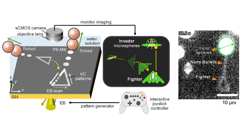
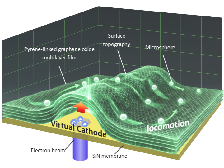
To overcome these limits, the first author, Ken Sasaki, and Associate Professor Hisataka Maruyama, along with Professor Takayuki Hoshino of Nagoya University’s Graduate School of Engineering, combined two innovative technologies. The first is a “virtual cathode” display, in which an electron beam is scanned across a silicon nitride (SiN) membrane along a computer-defined path, generating a localized electric field with nanoscale precision. Because the pattern is set by the scan path rather than a physical electrode, its shape and position can change instantly.
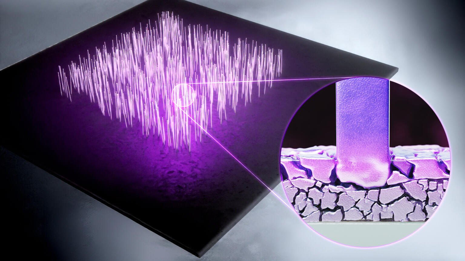
The second is a multilayer film of pyrene-linked graphene oxide, about 45 nanometers thick and made of roughly 29 stack layers, anchored to the SiN membrane. Because the film carries a negative surface charge in water, exposure to the beam’s charged region induces electrostatic repulsion against the SiN layer. This slides the stacked layers apart slightly, then peels the bottom layer away from the membrane, bulging the film into a dome.
Observing nanoscale changes
Graphene oxide normally does not fluoresce, because tightly stacked sheets quench each other’s fluorescence. As the beam was applied, the film’s fluorescence switched on and intensified — a sign that the layers were separating and the quenching was being relieved. As the film bulged, the changing water-layer thickness beneath it produced interference patterns resembling contour lines, allowing the team to measure otherwise invisible height changes in real time.
Key experimental findings
A dome-shaped bump roughly 1,200 nanometers high and 37 micrometers across formed within 10 seconds, which is significantly faster than light-based methods and matches the speed of the fastest electrical systems reported, but with a much larger height change.
The deformation was reversible but asymmetric: the film swelled at 100–200 nanometers per second but subsided at only 40–55 nanometers per second once the beam was off, so full recovery took 20 seconds or more. The team attributes this to the SiN membrane’s dielectric polarization building up quickly under the beam, while the residual surface charge dissipates far more slowly.
By adjusting beam exposure time and current, and by moving the beam to merge adjacent deformed regions, the researchers reshaped domes into larger domes or valley-like depressions, and the film retained its structure after repeated reconfiguration at the same spot.
As a proof of concept, the bulge pushed a single 10-micrometer polystyrene bead through water in a controllable direction, with an estimated mechanical pushing force of 0.05 piconewtons and a separate electrostatic repulsion of 0.11 piconewtons — suggesting, but not yet demonstrating, potential for moving cells or powering microscopic robots.
Outlook
“We believe this technology will facilitate integration between nanomachines and computers,” Hoshino said. “Nano- and micro-scale irregularities at interfaces are crucial for friction and adhesion between objects. This display technology can generate these irregularities on demand, which we hope will eventually enable control over the adhesion and assembly of microscopic cells and objects.”
The researchers note that precisely controlling where the film delaminates, and demonstrating stable operation in physiological electrolyte rather than pure water, remain open challenges before living cells can be manipulated this way.
Paper information
Ken Sasaki, Hisataka Maruyama, and Takayuki Hoshino, 2026. Electric Field-Driven Dynamic Surface Topography of Pyrene-Linked Graphene Oxide Multilayer Film, ACS Applied Materials & Interfaces
DOI: 10.1021/acsami.5c22563
Funding information
This work was supported by research grants from JSPS KAKENHI (grant numbers 22K18775 and 23KJ0078) and the JKA Foundation (grant number 2024M-563).
Expert contact
Takayuki Hoshino
Nagoya University Graduate School of Engineering
Email: hoshino.takayuki.v7@f.mail.nagoya-u.ac.jp
Media contact
Naomi Inoue
Nagoya University International Communications Office
Email: icomm_research@t.mail.nagoya-u.ac.jp
Top image
An electron beam creates a “virtual cathode” that reshapes a graphene oxide nanofilm into on-demand 3D surface features, capable of pushing microscopic beads in a controlled direction.
(Credit: Ken Sasaki)