Nagoya University researchers develop first GeSn-based Group IV resonant tunneling diode that operates at room temperature.
In a world first, researchers at Nagoya University in Japan have successfully developed a resonant tunnel diode (RTD) that operates at room temperature made entirely from Group IV semiconductor materials. The development of an RTD that operates at room temperature means the device could be deployed at scale for next-generation wireless communication systems. The use of only non-toxic Group IV semiconductor materials also supports more sustainable manufacturing processes.
This research marks a pivotal step toward terahertz wireless components that deliver unprecedented speed and data handling capacity with superior energy efficiency. “Compared to InGaAs-based Group III-V RTDs that include toxic and rare elements, such as indium and arsenic, Group IV compounds-based RTDs are safer, lower cost, and offer advantages for creating integrated production processes,” said senior author Dr. Shigehisa Shibayama from the Nagoya University Graduate School of Engineering. The results were published in the journal ACS Applied Electronic Materials.
Terahertz waves and quantum devices
Researchers have long struggled to achieve the high-speed and large-volume data transfer needed for sixth-generation (6G) cellular networks. One promising solution is wireless communication using terahertz waves—electromagnetic waves that vibrate a trillion times per second, enabling ultra-high-speed data transmission. However, many technical challenges remain before this technology can be made practical for consumer applications.
A critical component for realizing terahertz communication is the RTD. This quantum device operates through negative differential resistance, a counterintuitive property where increasing voltage actually decreases current. When part of a properly designed circuit, this property allows the diodes to sustain high-frequency oscillations that would otherwise decay due to electrical losses.
Moving beyond laboratory constraints
The secret behind an RTD lies in its double-barrier structure, where electrons or holes tunnel through layers of different semiconductor materials, each only a few atoms thick. These layers have mainly been created from InGaAs-based Group III-V materials that include toxic and rare elements, such as indium and arsenic.
In previous research by the same group, the researchers created a p-type RTD using only Group IV materials, specifically germanium-tin (GeSn) and germanium-silicon-tin (GeSiSn) alloys. One limitation was that the diode only functioned at extremely low temperatures, around -263°C. Since consumer electronics and wireless systems cannot practically reach this level of cooling, the device would have remained a laboratory curiosity.
Shibayama and his colleagues have now discovered how to use only Group IV materials to produce a p-RTD that functions at room temperatures of around 27°C. This significant improvement opens new possibilities for the widespread adoption of terahertz semiconductor devices.
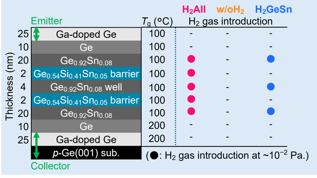
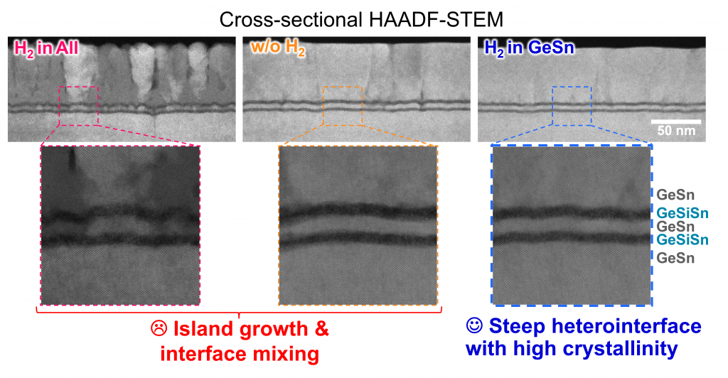
The research group achieved its breakthrough by introducing hydrogen gas during the layer formation process. They tested three different scenarios: 1) introducing hydrogen gas to both the two GeSiSn layers and three GeSn layers, 2) introducing no hydrogen gas, and 3) introducing hydrogen gas to only the three GeSn layers. In the last scenario, hydrogen gas restricted island growth and mixing between layers, resulting in a smooth and well-ordered double-barrier structure.
“The RTD cannot function if these layers are mixed,” said Dr. Shibayama. “If there are defects in the layers, electrons can tunnel through these easier routes, leading to current leakage. This leakage current needs to be reduced for negative differential resistance—the key property of an RTD—to occur.”
Publication:
Shota Torimoto, Shuto Ishimoto, Yoshiki Kato, Mitsuo Sakashita, Masashi Kurosawa,
Osamu Nakatsuka, & Shigehisa Shibayama. (2025). Room temperature operation of Ge1−xSnx/Ge1−x−ySixSny resonant tunneling diode featured with H2-introduction during molecular beam epitaxy. ACS Applied Electronic Materials, 7(16), 7688–7696. https://doi.org/10.1021/acsaelm.5c01049
Funding:
This research was supported in part by JST PRESTO (Grant Number JPMJPR21B6) and JST CREST (Grant Number JPMJCR21C2).
Expert contact:
Shigehisa Shibayama
Nagoya University, Graduate School of Engineering
s-shibayama@nagoya-u.jp
Media contact:
Alexander Evans
Nagoya University, International Communications Office
icomm_research@t.mail.nagoya-u.ac.jp
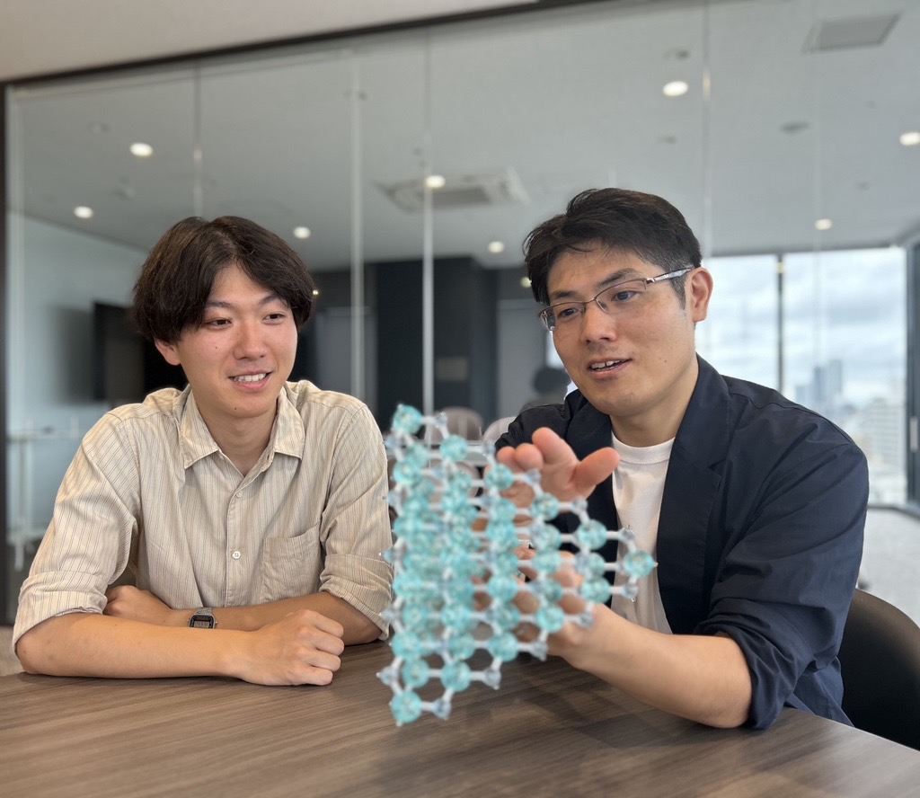
Top image: Assistant Professor Shigehisa Shibayama (right) and first author Shota Torimoto (left), along with the rest of the team, have developed a resonant tunneling diode using only non-toxic Group IV semiconductor materials that operates at room temperature. Credit: Shigehisa Shibayama (Nagoya University) and Shota Torimoto (Nagoya University)