This technique also eliminates the need for fluorocarbon gases, which have significant global warming potentials.
After more than a decade of research and development, Tokyo Electron Miyagi Ltd. has introduced an innovative semiconductor etching method that achieves etch rates up to five times faster than conventional processes. Now, a collaborative research team from Nagoya University and the company has examined the underlying etching mechanisms responsible for this enhanced performance.
This new method employs plasma etching with hydrogen fluoride (HF) at very low temperatures. In contrast to conventional fluorocarbon etching gases, which have high global warming potentials (GWPs), HF has a substantially lower GWP.
The study demonstrated that this process significantly reduces processing time and enhances energy efficiency, particularly for etching complex three-dimensional (3D) structures in advanced devices, such as gate-all-around (GAA) transistors and 3D NAND flash memory chips. The findings were published in the Chemical Engineering Journal.
Semiconductor etching is an essential chip-manufacturing process that selectively removes material from a wafer surface to form precise circuit patterns. Reactive ion etching technologies have played a pivotal role in wafer fabrication through synergistic reactions between chemical gases and ions.
However, ongoing miniaturization of semiconductor devices poses substantial challenges for etching techniques, especially in delivering chemical species deep into complex 3D structures with high aspect ratios, where the depth is much greater than the width. These difficulties have led to a considerable decrease in “etching throughput,” the amount of etching work done in a particular period of time.
To address these challenges, a Nagoya University research team, led by Professors Shih-Nan Hsiao and Masaru Hori of the Center for Low-temperature Plasma Sciences, collaborated with Tokyo Electron Miyagi Ltd., a manufacturer of plasma etching equipment, to verify that this new etching process mechanism significantly enhances throughput.
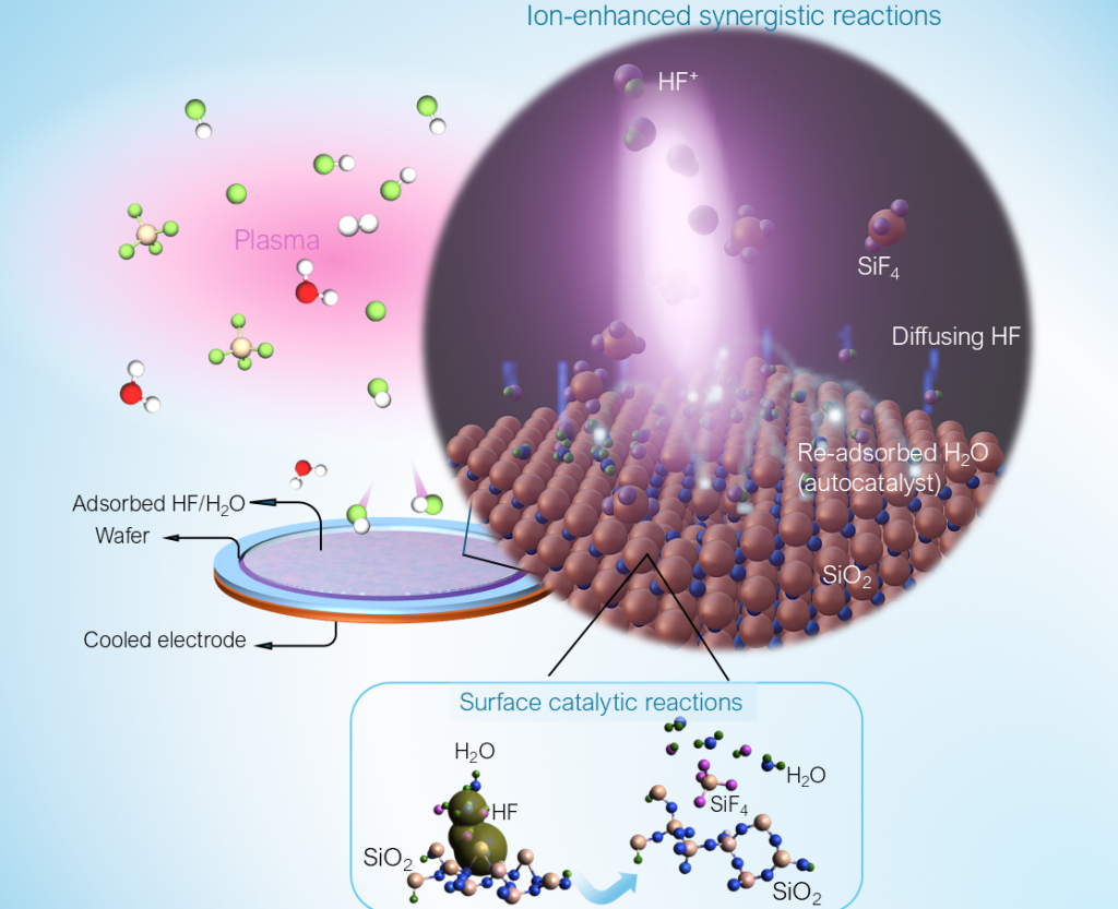
Previous studies have indicated that cooling the substrate to ultra-low temperatures substantially increases etch rates in silicon-based materials, such as silicon dioxide (SiO₂) films. Furthermore, it has been suggested that co-absorption of HF and the etching reaction product, water (H₂O), significantly enhances surface reactions at very low temperatures.
“However, precise synergistic interactions between HF ions, surface-adsorbed HF and H₂O, and the material surface being etched for cryogenic plasma etching remain unclear,” stated Professor Hsiao. “Therefore, we assessed the performance of etching SiO₂ films using HF plasma at very low temperatures.”
The researchers cooled the semiconductor substrate to −60°C and then exposed it to an HF plasma. They observed that both HF and H₂O adsorbed onto the SiO₂ surface and found that H₂O acts as a catalyst, reducing the etching activation barrier to nearly zero.
The study also demonstrated that increasing ion irradiation energy promotes the generation of H₂O, which subsequently adsorbs onto the surface, accelerating a self-catalytic cycle that attracts HF. Interestingly, this process, referred to as an ion-enhanced surface autocatalytic reaction, resulted in an exponential increase in the film etching rate per unit of ion energy.
The study confirmed that this new process achieves an etching throughput for SiO₂ films approximately 100 times greater than that attained under conventional room-temperature and low-ion-energy conditions.
“Furthermore, the use of HF plasma instead of conventional fluorocarbon gases, which typically exhibit high global warming potentials, eliminates the carbon footprint associated with the etching process,” stated Professor Hsiao.
“Through this industry collaboration, we are advancing verification in an environment similar to actual manufacturing equipment. We aim to apply this process to semiconductor manufacturing lines and extend its use to broader production processes.”
Paper information:
Shih-Nan Hsiao, Yusuke Imai, Makoto Sekine, Ryutaro Suda, Yuki Iijima, Yoshihide Kihara, Kenji Ishikawas, and Masaru Hori (2025). Revolutionizing reactive ion etching: ion-enhanced surface autocatalytic reactions enabling ultra-high throughput using cryogenic hydrogen-fluoride plasma. Chemical Engineering Journal.
DOI: 10.1016/j.cej.2025.167517
Expert contact:
Shih-Nan Hsiao
Center for Low-temperature Plasma Sciences
Email: hsiao.shih.nan.t8@f.mail.nagoya-u.ac.jp
Media contact:
Naomi Inoue
International Communications Office, Nagoya University
Email: icomm_research@t.mail.nagoya-u.ac.jp
Top image:
Synergy of ion-enhanced and surface adsorbed HF/H2O for etching
(Credit: Shih-Nan Hsiao)