Thermoelectric crystal reveals a record-high conductivity resulting from its peculiar charge carrier properties at low temperatures
Just as a voltage difference can generate electric current, a temperature difference can generate a current flow in thermoelectric materials governed by its "Peltier conductivity" (P). Now, researchers from Japan demonstrate an unprecedented large P in a single crystal of Ta2PdSe6 that is 200 times larger than the maximum P commercially available, opening doors to new research avenues which can potentially revolutionize modern electronics.
We all know that current flows inside a metallic conductor in presence of a voltage difference across its ends. However, this is not the only way to generate current. In fact, a temperature difference could work as well. This phenomenon, called "Seebeck effect," laid the foundation of the field of thermoelectrics, which deals with materials producing electricity under the application of a temperature difference.
Similar to the concept of an electrical conductivity, thermoelectricity is governed by the Peltier conductivity, P, which relates the thermoelectric current to the temperature gradient. However, unlike its electrical counterpart, P is less explored and understood. For instance, is there a theoretical upper limit to how large P can be? Far from being a mere curiosity, the possibility of a large P could be a game changer for modern-day electronics.
A new study published in the Journal of Physics: Energy has raised hopes on this front, reporting the observation of a P of 100 A cm-1 K-1 at a temperature of 10 K in a Ta2PdSe6 crystal, the largest ever reported for a bulk solid. "Ta2PdSe6 is structurally similar to Ta2NiSe5, a material which we found shows unique structural and transport properties. This led us to focus on the properties of Ta2PdSe6 and we ended up discovering the giant Peltier conductivity," explains Assistant Professor Akitoshi Nakano from Nagoya University, Japan, who led the research team conducting this study.
The team prepared high-quality single crystals of Ta2PdSe6 and characterized its chemical composition using scanning electron microscopy with energy dispersive x-ray spectroscopy and x-ray diffraction. Next, they measured its electrical conductivity, thermopower, and Hall resistivity and performed calculations based on a two-carrier model considering electrons and holes (the absence of electrons, represented by particles with a positive charge equal to the electronic charge) to explain their findings.
They found that while other thermoelectric materials reached a P of the order of 1 A cm-1 K-1 at best before going down as the temperature decreased further, Ta2PdSe6 showed a rapid growth in P below 100 K, reaching a value higher by two orders of magnitude! This suggested that the large P stemmed from a low residual resistivity.
The modeling calculations revealed that the surprising P value was caused by the high mobility, low concentration, and heavy mass of the holes inside the crystal.
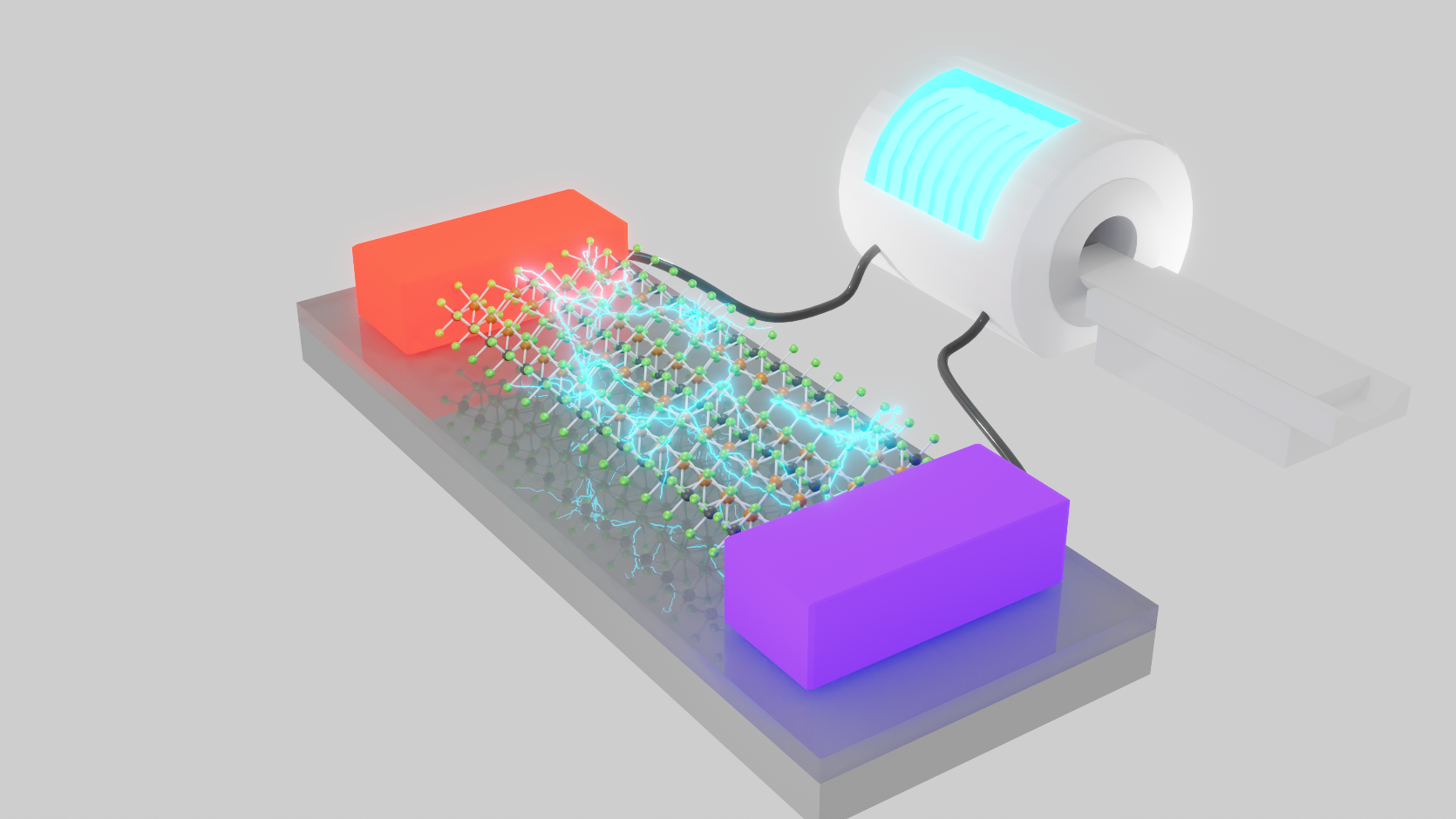
What practical ramifications could this finding entail? "Ta2PdSe6 could be used as a current source for a superconducting solenoid isolated in a cryogenic space. Due to its large P, a cubic sample of 1 cc could supply a current of 100 A to the solenoid for a temperature difference of 1 K. Furthermore, an absence of external current leads would make the system compact and concise, reducing cooling costs," says Dr. Nakano. "This could be then carried over to the design of a compact, low-cost MRI machine, making medical diagnosis more convenient in the future."
We certainly hope his visions will be realized soon!
The paper, "Giant Peltier conductivity in an uncompensated semimetal Ta2PdSe6," was published in Journal of Physics: Energy on September 15, 2021, at DOI: 10.1088/2515-7655/ac2357.
Authors
Akitoshi Nakano1, Ai Yamakage1, Urara Maruoka1, Hiroki Taniguchi1, Yukio Yasui2 and Ichiro Terasaki1
1 Department of Physics, Nagoya University
2 Department of Physics, Meiji University
Media Contact
Akitoshi Nakano
Graduate School of Science, Nagoya University
Email: nakano.akitoshi@nagoya-u.jp
Funding
Kakenhi Grant No. 19H05791, 20K20898, and 21K13878 of Japan