Surfaces play a key role in numerous chemical reactions, including catalysis and corrosion. Understanding the atomic structure of the surface of a functional material is essential for both engineers and chemists. Researchers at Nagoya University in Japan used atomic-resolution secondary electron (SE) imaging to capture the atomic structure of the very top layer of materials to better understand the differences from its lower layers. The researchers published their findings in the journal Microscopy.
Some materials exhibit ‘surface reconstruction’, where the surface atoms are organized differently from the interior atoms. To observe this, especially at the atomic level, surface-sensitive techniques are needed.
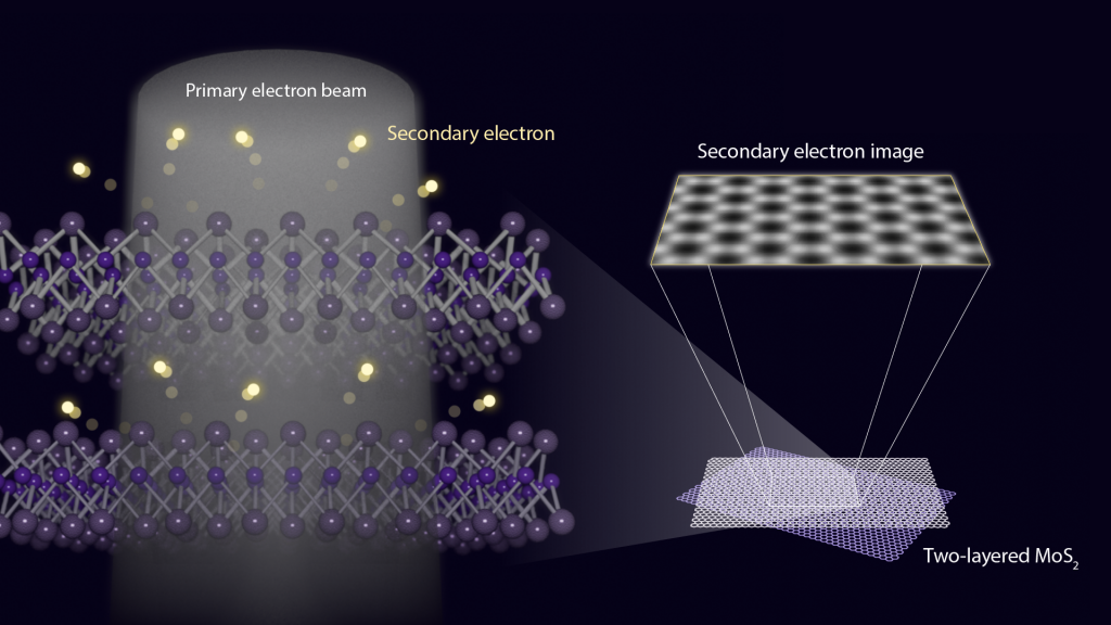
Traditionally, scanning electron microscopy (SEM) has been an effective tool to examine nanoscale structures. SEM works by scanning a sample with a focused electron beam and capturing the SEs emitted from the surface. SEs are typically emitted from a shallow depth below the surface, making it difficult to observe phenomena like surface reconstruction, especially if only a single atomic layer is involved.
The Nagoya University research team tackled this issue using the simplest workable system, a two-layered molybdenum disulfide (MoS₂) sample, to measure how much information SE imaging can extract from the surface and subsurface layers. By stacking two layers of MoS₂, they distinguished the surface layer from the second layer using the technique.
The researchers found that atomic resolution SE imaging is effective in identifying surface atomic arrangements with extremely high surface sensitivity. Their findings revealed that the intensity of SE images from the surface layer was about three times higher than from the second layer, providing strong evidence of the method’s sensitivity.
Atomic-resolution SE images of a single-layer MoS₂ sample revealed stunning honeycomb-like structures composed of molybdenum and sulfur atoms. Beyond its visual appeal, SE imaging revealed overlapping patterns, indicating distinct atomic arrangements in the surface and second layers.
“Most notably, the SE yield from the surface layer was about three times greater than from the second layer,” Koh Saitoh, lead author and researcher at Nagoya University’s Institute of Materials and Systems for Sustainability (IMaSS), explained. “This result suggests that the surface layer absorbs or scatters SEs from the second layer. This absorption contributes to the method’s depth sensitivity.”
The aim of the group is to use atomic resolution SE imaging to reveal the surface structure at the atomic level, including surface reconstruction and other unique structures formed on surfaces. To control the growth, fabrication, and electronic and mechanical properties of nanomaterials, understanding these processes is essential.
The study, “Surface sensitivity of atomic resolution secondary electron imaging,” was published in the journal Microscopy on September 20, 2024, at DOI: 10.1093/jmicro/dfae041.
Authors
Koh Saitoh, Teppei Oyobe, Keisuke Igarashi, Takeshi Sato, Hiroaki Matsumoto, Hiromi Inada, Takahiko Endo, Yasumitsu Miyata, Rei Usami, Taishi Takenobu
Media Contact
Matthew Coslett
- International Communications Office, Nagoya University
- Email: icomm_research@t.mail.nagoya-u.ac.jp
Top image: Secondary electrons (SEs) emitted from the surface layer are detected by the SE microscopy whereas the SEs from the bottom layer are absorbed or scattered by the surface layer. (Credit: Reiko Matsushita)