Researchers from Nagoya University in Japan have found that depositing an ultrathin (less than 10 nanometers) magnesium layer onto gallium nitride (GaN), then gently heating it for a short time, creates the best electrical contacts yet reported for the thin p-type layers used in devices such as LEDs and power transistors.
Semiconductor devices such as LEDs and transistors are generally made up of two halves: an n-type which carries negative charge via electrons, and a p-type which moves positive charge carriers called holes that are essentially electron-voids. Both halves rely on contacts that can get electric current in and out of them with minimal loss of energy. These connections, known as ohmic contacts, have been an efficiency bottleneck in thin p-type GaN semiconductors for decades owing to their high resistance.
Now, a team led by Haitao Wang and Jia Wang at the Institute of Materials and Systems for Sustainability (IMaSS), Nagoya University, has come up with a new way of lowering the resistance of p-type GaN contacts. They deposited an ultrathin magnesium layer onto the p-GaN surface and gave it a heat treatment at 600 degrees Celsius for five minutes, thereby achieving a contact resistivity of (1–3) × 10⁻⁴ Ω cm² without damaging the surface. This is among the lowest reported contact resistivities for thin p-type GaN.
Their findings, which are expected to make a wide range of electronic devices used in places such as electric vehicles and data centers more energy-efficient, have been published in the journal Applied Physics Letters.
The challenges of p-GaN contacts
Magnesium-doped p-type GaN was developed at Nagoya University by Isamu Akasaki and Hiroshi Amano in work recognized by the 2014 Nobel Prize in Physics for blue LEDs. In this material, holes are produced by adding small quantities of magnesium, which has one fewer valence electron than the surrounding gallium, in a process known as doping.
However, magnesium is a stubborn acceptor of electrons at room temperature. As a result, the metal-semiconductor boundary does not have enough mobile holes, resulting in a wide barrier called a depletion region. This barrier creates high resistance to the flow of charge and thus more energy is needed to drive currents across it.
One way to counter this high resistivity is to grow a heavily doped GaN layer with rich concentration of holes right at the interface. But this is a costly and laborious process that is vulnerable to damage under later device fabrication stages such as plasma etching.
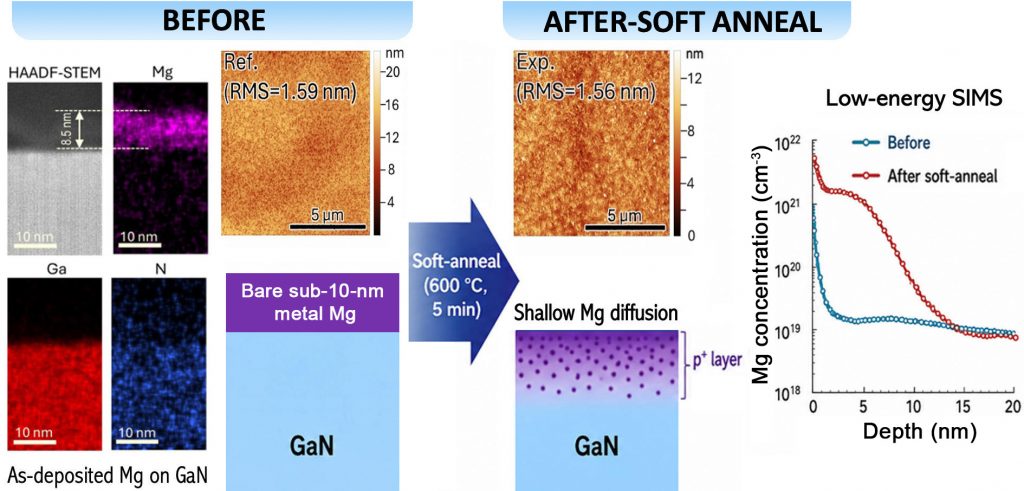
A thin magnesium layer does the job, no cap!
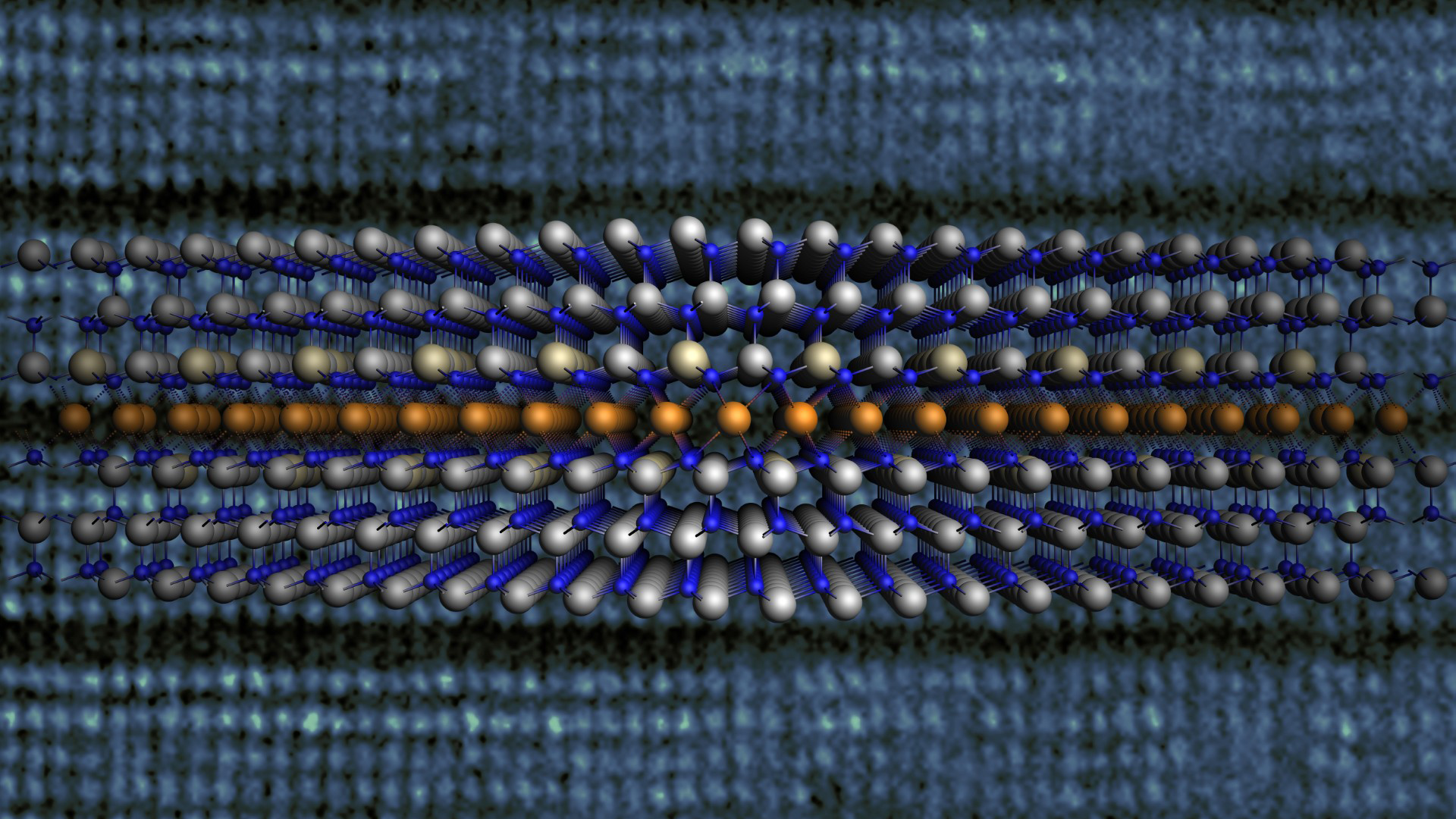
To look for alternatives, a few years earlier, the same group tried depositing a layer of metal magnesium directly onto a GaN wafer and processed it with a heat treatment called annealing. This magnesium layer was relatively thick, measuring dozens of nanometers. In doing so, they also discovered the emergence of a remarkable superlattice structure.
“This superlattice was very interesting for fundamental science,” said Jia Wang, who led the 2024 study published in Nature. “But at that time, the surface after annealing was too rough, raising concerns about device reliability particularly for thin p-type GaN, so some of the benefits of this approach could not be fully demonstrated.”
To solve the roughness issue, Haitao Wang pivoted to depositing a much thinner magnesium film. The problem with this is magnesium’s high reactivity that makes it oxidise easily in air. To prevent this, a protective cap layer is typically used to isolate the magnesium from air. But all samples using a cap showed unwanted impurities.
“I then tried [a capless sample] as a reference, and it came out as a surprise,” Haitao Wang said. “I found that the cap didn’t make any difference.” It it likely that only the very top layer of magnesium gets oxidized, preserving the rest even if the total thickness is no more than 10 nanometers.
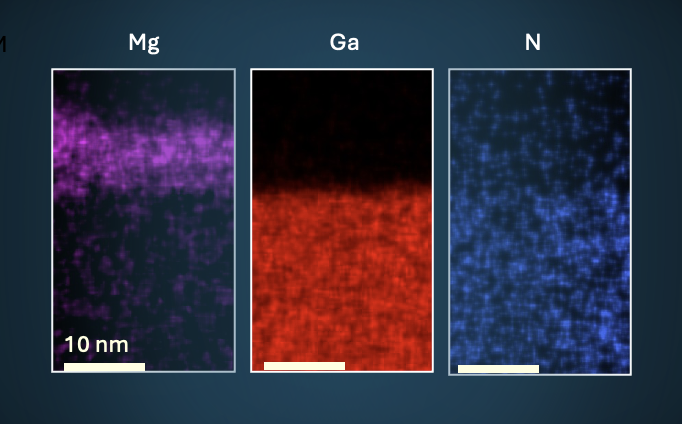
The researchers subjected this thin layer to a heat treatment called “soft annealing,” where the sample is heated to a lower temperature (600 degrees Celsius) and for a shorter time (five minutes) compared to normal annealing. During this process, the ultrathin magnesium layer gets rapidly consumed as the magnesium diffuses into the surface region of the p-type GaN. To the researchers’ delight, this new surface turned out to be much smoother than in their previous work.
This ultrathin, ultrahigh concentration mangesium doped layer narrowed down the contact depletion region and promoted tunneling of holes across it, thereby lowering contact resistance.
Further, this ‘top-down’ process is a lot simpler, quicker, and cheaper to implement than ‘bottom-up’ crystal growth. It can also be applied after device processing, making it more flexible and compatible with existing fabrication processes. As a result, it holds promise for accelerated commercialization of higher-efficiency semiconductors.
“We are now applying this method to different types of devices like LEDs and transistors in electric vehicles,” said Wang.
Publication information:
Haitao Wang, Shumeng Yan, Zhiyu Xu, Yingying Lin, Peirong Yu, Joshua Jaehyung Park, Joseph E. Dill, Hei Wong, Qingyuan Han, Xigen Li, Qian Sun, Tomás Palacios, Debdeep Jena, Huili Grace Xing, Jia Wang, Hiroshi Amano, 2026. Enabling thin p-GaN Ohmic contacts through ultrathin magnesium deposition and brief thermal annealing. Appl. Phys. Lett. DOI: https://doi.org/10.1063/5.0339815
Funding information:
This work was supported by the Japan Science and Technology Agency (JST) Adopting Sustainable Partnerships for Innovative Research Ecosystem (ASPIRE) program (Grant No. JPMJAP2311), the Japan Society for the Promotion of Science (JSPS) Grants-in-Aid for Scientific Research (KAKENHI, Grant No. 24K17305), and the Young Researchers Activation Support Project of the Center for Integrated Research of Future Electronics (CIRFE), Nagoya University.
Expert contacts:
Jia Wang
Institute for Advanced Research,
Institute of Materials and Systems for Sustainability (IMaSS),
Nagoya University
Email: wang.jia.t4@f.mail.nagoya-u.ac.jp
Haitao Wang
Institute of Materials and Systems for Sustainability (IMaSS),
Nagoya University
Email: wang.haitao.t8@f.mail.nagoya-u.ac.jp
Media contact:
Sumeet Kulkarni
International Communications Office
Nagoya University
Email: icomm_research@t.mail.nagoya-u.ac.jp
Researchers

Related organizations
Related tags
- Efficiency
- Gallium nitride
- GaN
- High quality GaN
- LEDs
- Magnesium
- Mathematical and physical sciences
- P-type semiconductors